Semiconductors and plasmonic nanomaterials can be coupled to develop photocatalytic and detection systems. Nanoscale composites containing semiconductors and metals can improve plasmon-assisted spectroscopy and boost catalytic performance by modulating the charge states of the metals.
Study: Hybrid composite based on conducting polymers and plasmonic nanomaterials applied to catalysis and sensing. Image Credit: GiroScience/Shutterstock.com
An article published in Materials Research Express showed an enhancement in Raman scattering by using conductive polymers as semiconducting platforms.
An Introduction to Raman Spectroscopy
Vibrational spectroscopy is a method for determining the molecular framework caused by particles' vibrational oscillations. Raman scattering is a popular vibrational spectroscopy technique.
The Raman signal produces a distinct spectrum for molecules and is beneficial for analytical purposes. However, Raman scattering has weaknesses and requires considerable improvement before its widespread use in analytical studies can be realized.
In the spectroscopy technique, only one out of every 106 photons is transformed into Stokes Raman scattering, resulting in inadequate strength of the analytical signal. The introduction of nanostructures may enhance the Raman effect using plasmonic amplification, allowing for Raman sensing of singular molecules.
Nanostructured materials may be created using advanced material processing and characterizing techniques, including metallic nanostructures with various morphologies and characteristics.

Figure 1. (a) FTIR spectra of the treated and nontreated P3HT: PCBM also showed different temperatures of 50, 100, 150, 200, and 250 °C in the oven for 40 min (b) fluorescence spectra of P3HT: PCBM before and after thermal annealing at 250 °C. (c) The water contact angle of the blended P3HT: PCBM shows different temperatures of 0 to 250 °C. (d) ) SEM images of (i) Ag NPs 40 nm size (ii) P3HT. (iii) PCBM. (iv) P3HT:PCBM/Ag NPs.
Enhancing Raman Scatter
A significantly amplified electromagnetic (EM) field is generated on the metallic nanostructure surfaces by excitation of localized surface plasmons. A chemical process or an EM technique may improve the Raman effect.
The chemical process has received less attention because of its lower Raman amplification effects compared to those of EM origin. Charge transference activities in the molecule-platform complex, like those caused by derivative resonance coupling, enhance the Raman effect signals.
Photo-Induced Enhanced Raman Spectroscopy
It is possible to achieve surface-enhanced Raman scattering (SERS) by combining photo-triggered oxygen vacancy defects on the surface of semiconducting materials like TiO2.
The oxygen vacancy states were shown to promote derivative couplings among semiconducting materials, defects, metals, and analytes. These couplings, in turn, enhance the Raman effect. The mechanism was dubbed photo-induced enhanced Raman Spectroscopy, or PIERS, for short.
PIERS can be used for detecting minute amounts of different small-molecule analytes for a variety of semiconducting materials. Along with PIERS methods, semiconducting materials may build junctions between metals and themselves, allowing efficient carrier segregation via a Schottky junction.
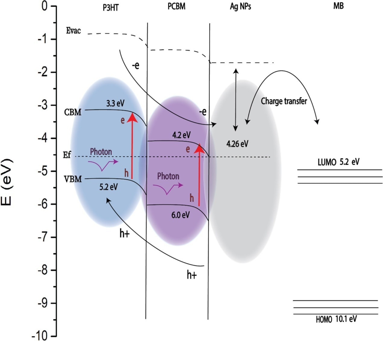
The Schottky junction is generated when the semiconducting material and metal come into close proximity, and the charge carriers traverse from one part to the other, which helps in bringing their Fermi levels to an equilibrium.
Figure 2. SERS spectra of 4-nitrophenol (4NP) recorded on P3HT: PCBM (a) SERS recorded on polymer blends that were annealed at different temperatures. (b) normalized SERS intensity prior (black) following (red) heat treatment. (c) Schematic of the oxidation reaction and formation of 4-aminophenol from 4-Nitrophenol.
Which Semiconductor Was Used in the Study?
A combination of n-type and p-type semiconducting materials, such as P3HT: PCBM, is a commonly utilized conductive organic semiconductor.
The P3HT polymer exhibits great charge movement in highly crystallized sheets and serves as a donor of electrons in the photo-excitation phase. Exciton breakdown is made possible by the complementary PCBM. When used with gold (Au) or silver (Ag) nanoparticles, the P3HT: PCBM polymer combination creates a Schottky junction.
Research Methodology
As a framework for improving the Raman effect, P3HT: PCBM and Ag nanoparticles were blended in this work. The team showed that heat treatment of this semiconducting-plasmonic complex significantly improved the surface-enhanced Raman spectroscopy signal that analytes may generate. Moreover, the team demonstrated that the polymeric complex supports the plasmonic catalytic processes.
The team also examined the photoluminescence (PL) spectra of the polymeric complex. They measured the contact angle for the different specimens before and after heat treatment.
Figure 3. An energy band diagram illustrating the electronic transition between P3HT: PCBM and Ag NPs and the MB analyte molecule. The red lines show electron transitions excited by the Raman excitation laser.
Important Findings of the Study
In this study, the team showed how the signal intensity of PIERS was enhanced approximately five-fold through the employment of conductive polymeric materials having plasmonic properties. Supporting mechanisms based on charge transference were found to encourage the oxidation of desired molecules on active plasmonic nanostructures.
Heat treatment of the polymeric mix enhanced the impact of self-trapped localized excitons on photoluminescence.
Using an optimized chemical mechanism, the charge transfer-based approach enhanced the Raman effect signals. The study showed how conductive polymers might be used as semiconducting frameworks for plasmonic catalysis and detection.
Reference
Alanazi, A. T., & Rice, J. H. (2022). Hybrid composite based on conducting polymers and plasmonic nanomaterials applied to catalysis and sensing. Materials Research Express. Available at: https://iopscience.iop.org/article/10.1088/2053-1591/ac7d9a


 Add Category


