


 Add Category


Nanophotonics is the study of light-matter interactions between light and objects on the nanometer scale. The length scales involved in nanophotonics are of such great scientific interest because this scale's objects give us access to new optical properties and functionalities that are not available in bulk materials.
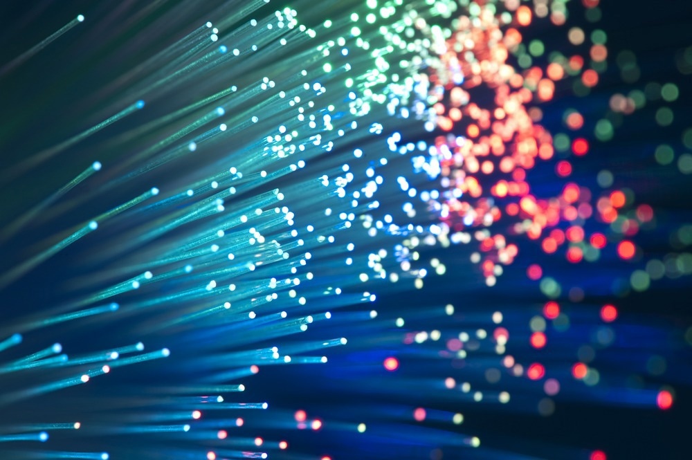
Image Credit: asharkyu/Shutterstock.com
Examples of nanophotonic devices include photonic crystals, waveguides, nanoantennas. Many nanophotonic devices are made from dielectric or metallic structures, where the device is structured to enhance to promote the light-matter interactions of interest. Often, these involve creating plasmonic resonances that can be manipulated to enhance signal levels in sensing and spectroscopy experiments.
Key application areas of nanophotonics include sensing, with point-of-care medical diagnostics being an area of particular growth, display technologies and optoelectronics or photovoltaic devices. As well as manufactured devices, there are examples of nanophotonic structures in the natural world, including butterfly wings and peacock features that are examples of photonic crystals containing nanoparticle assemblies.
Nanophotonic Technologies in Medical Devices
Nanophotonics can be used either for offline medical devices for biosensing, such as detecting specific DNA aptamers to identify a particular disease, or for point-of-care devices. For biosensing applications, the nanophotonic device reads a change in a signal when a particular biomarker is bound.
Often, nanophotonic biosensors make use of a change in the optical response on binding the biomarker as the detectable signal. Integrating nanophotonic technologies can help by boosting the signal levels associated with the binding event and improving the sensitivity so even trace amounts of biomarkers can be detected.
Point-of-care diagnostics involves using portable devices that can be used for diagnostics directly on the patient. Many devices circumvent the need for painful biopsies and can be interfaced with algorithms for automated analysis and diagnosis. With many point-of-care devices being much more straightforward to use than skilled medical procedures like biopsies and not requiring clinicians for full diagnosis, nanophotonic-based point-of-care devices are a good way of improving efficiency in healthcare. Such devices also present opportunities for healthcare in non-clinical settings.
Other examples of nanophotonic devices in medical settings include nanophotonics for rapid COVID-19 diagnostics and detection of gram negative bacteria.
Using Nanophotonics to Control Light
Controlling and shaping the properties light is at the heart of optical applications. With the development of optoelectronics and optical communication, as well as a push for using light-based technologies in solar energy harvesting, finding ways to convert light to electricity efficiently has been a key focus for scientific and technological developments in the field of nanophotonics.
Silicon-based devices are still the most popular and widely used of the available solar cell technologies and materials. While materials such as perovskites have boasted better efficiency gains since their initial development, silicon-based solar cells have proved the most practical and viable technology so far.
Nanophotonics structures are now being integrated into solar cells, particularly metallic nanoparticles, to enhance their light collection efficiencies and develop plasmonic solar cells. Metal nanoparticles can now be fabricated relatively cheaply and their broad, strong absorption spectrum across a wide range of the solar spectrum makes them ideal for photovoltaics.
Nanostructuring of solar cells is another way to improve light trapping efficiencies and structures such as nanowires and nanoparticles can help improve light management. Efficiency gains are key in being able to thin down solar cell devices as well as make smaller device areas feasible.
Other applications of nanophotonics in light control include the development of metalens technologies that allow for unprecedented levels of control of light focusing, polarization and other properties. Metalenses can be much more compact than traditional optics and designed to avoid the creation of aberrations in the beam with great promise for device miniaturization in applications such as spectroscopy and sensing or even in the fabrication of nanophotonic devices
What Does the Future Look Like for Nanophotonics?
One of the biggest challenges has been the fabrication of nanophotonic devices themselves. Creating nanometer-scale objects requires manufacturing techniques that work at the nanoscale with nanometer accuracy and precision.
Methods such as focused ion beam lithography combined with electron microscopy approaches that have sufficient spatial resolution to visualize components have been essential in creating some of the complex architectures required for fully exploiting nanophotonic effects.
Many nanophotonic devices are now created with a bottom-up approach using ion beam deposition to create the structure layer by layer. With the use of interferometers for the position stability of the ion sources and focusing optics on achieving focused beam sizes of < 10 nm, creating complex nanophotonic structures is becoming increasingly routine, but there are still many challenges to be overcome.
Direct laser writing is another approach for nanophotonic fabrication that makes use of lasers with high peak powers and photoresists. While many structures, including complex chiral materials, have been created with this approach, direct laser writing still faces the same challenge as focused ion beam manufacture of very slow write speeds.
The possibilities of orders of magnitude of signal enhancement for sensing applications have driven much of the development in nanophotonics and will continue to push manufacturing approaches to fully exploit the possibilities offered by sensors capable of detecting just single molecules.
Nanophotonics; A Game-Changer for Biosensing
References and Further Reading
Dastmalchi, P., A. Haddadpour, and G. Veronis. 2014. Nanophotonics: Devices for Manipulating Light at the Nanoscale. Woodhead Publishing Limited. http://dx.doi.org/10.1533/9780857098757.376
Starkey, Tim, and Pete Vukusic. 2013. “Light Manipulation Principles in Biological Photonic Systems.” Nanophotonics 2(4):289–307. https://doi.org/10.1515/nanoph-2013-0015
Anker, J. N., Hall, W. P., Lyandres, O., Shah, N. C., Zhao, J., & Duyne, R. P. Van. (2008). Biosensing with plasmonic nanosensors. Nature Materials, 7, 442–453. https://doi.org/10.1038/nmat2162
Yager, P., Domingo, G. J., & Gerdes, J. (2008). Point-of-Care Diagnostics for Global Health. Ann. Rev. Biomed. Eng, 10, 107–144. https://doi.org/10.1146/annurev.bioeng.10.061807.160524
Ruiz-Vega, G., Soler, M., & Lechuga, L. M. (2021). Nanophotonic biosensors for point-of-care COVID-19 diagnostics and coronavirus surveillance. JPhys Photonics, 3(1). https://doi.org/10.1088/2515-7647/abd4ee
Jia, Baohua. 2015. “Nanophotonics Silicon Solar Cells : Status and Future Challenges.” Nanotechnology Review 4(4):337–46. https://doi.org/10.1515/ntrev-2015-0025
Luo, X. (2018). Plasmonic metalens for nanofabrication. Nat Sci Rev, 5(2), 137–138. https://doi.org/10.1093/nsr/nwx135
Manoccio, Mariachiara, Marco Esposito, Adriana Passaseo, Massimo Cuscun, and Vittorianna Tasco. 2021. “Focused Ion Beam Processing for 3D Chiral Photonics Nanostructures.” Micromachines 12:6. https://www.mdpi.com/2072-666X/12/1/6/htm