III-V semiconductor nanowires have intriguing material features, which facilitate the creation of advanced electronic and optoelectronic devices at the nanoscale. Especially, III-V nanowires display exclusive properties that do not occur in their bulk form, thanks to their unique nanostructure nature.
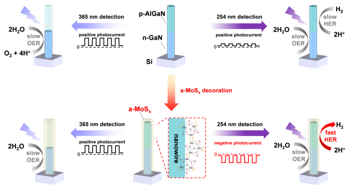
 Schematic illustration of the nanowire structures, operation of nanowire-based photoelectrochemical photodetectors under different light illumination, and the corresponding chemical reaction process at nanowire surface: Top: p-AlGaN/n-GaN nanowire; Bottom: a-MoSx decorated p-AlGaN/n-GaN nanowire. During operation, the photoresponse signal of the photoelectrochemical device is determined by the number of photo-generated carriers which effectively participate in the redox reactions, and the photocurrent polarity (either positive or negative) is determined by the type of predominate redox reaction triggered at solid/liquid interface. In other words, depending on the wavelength of the incident light, either hydrogen evolution reaction (HER) or oxygen evolution reaction (OER) will dominate in the photoelectrochemical photodetector, leading to the switch of photoconductivity. Image Credit: by Danhao Wang, Wentiao Wu, Shi Fang, Yang Kang, Xiaoning Wang, Wei Hu, Huabin Yu, Haochen Zhang, Xin Liu, Yuanmin Luo, Jr-Hau He, Lan Fu, Shibing Long, Sheng Liu, and Haiding Sun.
Such extraordinary one-dimensional (1D) geometry offers great openings to exploit their surface features (for instance, through surface decoration or alteration by a functional layer) to spur new occurrence which is hardly attainable in traditional nanowires, paving the path for the creation of advanced nanoscale electronic and optoelectronic systems.
A group of researchers, guided by Professor Haiding Sun, School of Microelectronics at the University of Science and Technology of China, and colleagues have integrated earth-copious molybdenum sulfides with the prevalent group III-nitride semiconductor nanowires to produce III-nitride/a-MoSx core-shell nanostructures which present positive photoresponsivity under 365 nm illumination and negative photoresponsivity under 254 nm illumination, which is seldom observed in conventional III-nitride nanowires.
Details of the study can be found in the journal Light Science & Application.
Photodetectors measure photon flux or optical power by converting the absorbed photon energy into electrical current, so-called photocurrent. In the operation of a photodetector, it is highly desirable that we can use the generated photocurrent, not only its magnitude but also its directionality to measure and diagnose the incident light signals. Consequently, once the photodetector demonstrates a dual-polarity photocurrent behavior upon different wavelength light illumination, we are able to distinguish different spectra bands,” said researchers.
Prof. Sun teamed up with other researchers, and they suggested the creation of III-nitride/MoSx core-shell nanowires for building spectrally intuitive photoelectrochemical photodetectors.
Such a monolithically incorporated core-shell nano-device construction not only resolves problems of the nanowire surface states but also increases the functionalities of the device by releasing the complete potential of the two types of low-dimensional materials.
Consequently, the novel a-MoSx/GaN core-shell nano-architecture boosts greater device performance, displaying an ideal positive photoresponsivity of 29.5 mA·W−1 under 365 nm illumination and negative photoresponsivity of -100.42 mA·W−1 under 254 nm, which signifies one of the leading devices among the well-known spectrally unique photosensors.
“This vertical nanowire p-n heterojunction configuration based photoelectrochemical device presents a new universal photodetector architecture with ultrabroad wavelength coverage and selectivity that can span ultraviolet, visible, and/or infrared spectral range by constructing nanowire p-n heterojunctions composed of any binary or ternary III-V semiconductors (III- nitrides, arsenides, and phosphides etc.). This is ascribed to the unique one-dimensional structure of nanowires, which allows sufficient strain relaxation for epitaxial growth of a broad range of lattice-mismatched materials.” they added.
“The presented technique can be used in multiple-band and spectrally distinctive photodetection in building modern light-induced sensing systems, including colorful and filter-less imaging, portable spectrometer, artificial vision, bio-sensors, and optically-controlled logic circuits.”
“Particularly, for those emerging photoelectrochemical-type (PEC-type) photodetectors, they can be directly implemented in aqueous condition, such as in bio blood environment, seawater, or underwater environment for light communication, photo-sensing and bio-detection, as compared with those conventional solid-state photodetectors that requires sophisticated packaging for aqueous application,” the scientists elucidate.
Wang, D., et al. (2022) Observation of polarity-switchable photoconductivity in III-nitride/MoSx core-shell nanowires. Light Science & Application. doi.org/ 10.1038/s41377-022-00912-7.
Source: http://english.ciomp.cas.cn/


 Add Category
